Electronic breakdown of multiwalled carbon nanotubes |
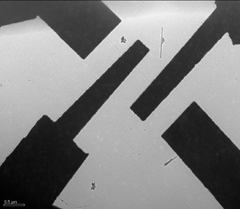
| Multiwalled carbon nanotubes fail in a step-wise fashion when subjected to extremely high electrical currents (Collins et al, Science 292 706). Electronic transport measurements obtained during failure show discrete current steps, from which it has been surmised that equal amounts of current are carried by each wall. To further investigate this failure mode (as well as the electronic transport of carbon nanotubes in general) we have developed a TEM transparent device architecture allowing unprecedented atomic resolution imaging of operating nanotube devices. |
|
|
|
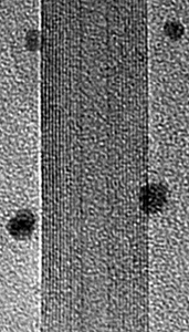
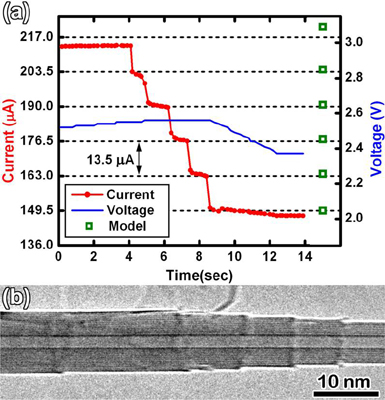
From our high resolution imaging we have confirmed the wall-by-wall failure mode suggested by the original report. However, we have also discovered that the equal current steps observed during breakdown cannot be attributed to the presence of equal amounts of current in each wall. To the contrary, we find that current is evenly distributed over the entire cross section of the nanotube, as if the nanotube were a macroscopic metal pipe. The electrical breakdown process can then be modeled by the removal of successively larger amounts of material from the outside of the pipe, as if by a lathe. We have confirmed this model in our experiments on shrinking nanotubes. |
|
|
|
(a) The current and voltage as a function of time during
electrical breakdown of a multiwalled carbon nanotube. The current
predicted at each step by our geometric model (the "lathe" model)
is shown by green squares on the right side of the plot.
|
|
See also: Featured in: |