- 4.19.
- 4.20. Consider 8-, 32-, and 64-bit words.
- What is the MTBF for the systems in 4.20? Consider both the mean time between detectable or correctable errors, and the mean time between true failures (what constitutes true failure of an ECC?).
Consider a microprocessor with a 32-bit memory bus, a 128Mbyte memory bank that is 4 bytes wide, and a simplified semi-synchronous bus cycle in which, in a no-wait bus cycle, there is a 0.5 clock period overhead, 2 clock periods for data access time, and a final 0.5 clock period overhead. Assume that the microprocessor requests one memory operation (read or write) per bus cycle. (See the figure.)
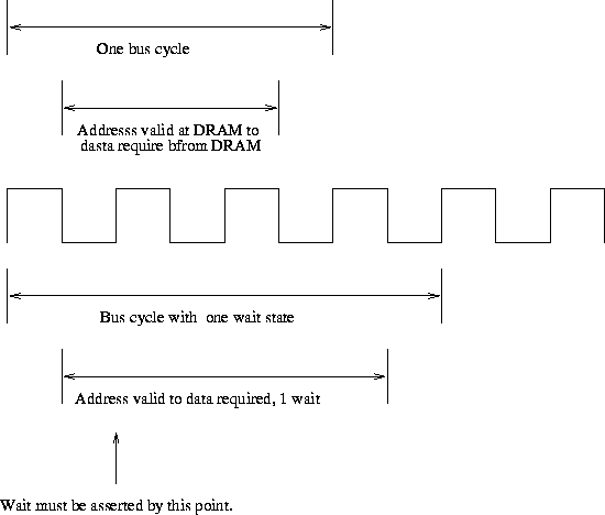
The interface logic drives the DRAM at its fastest possible speed, and all its delays are accounted for in the 1-clock overhead to the bus cycles.
- Design circuitry to decide whether or not page mode can be used
for each memory request. Design it so that it can be assumed to
correctly assert
 in 0.5 clock cycles. Use a databook to
find maximum delay times for your selected parts.
in 0.5 clock cycles. Use a databook to
find maximum delay times for your selected parts. - For a clock speed of 10MHz, how many wait states are needed without your circuit? How many for sequential and random addresses with your circuit? Thoroughly justify your answer, being sure that all timing constraints are met (the most important are likely to be access time and cycle time). An annotated timing diagram would help.
- For 25MHz?
- For 50MHz?
- Assuming the 50MHz clock, suppose that all memory accesses come in groups 4 sequential accesses (the microprocessor has a 4-word cache line). What is the memory bandwidth (Mbytes per second) with and without your circuit? What speedup did you gain?