
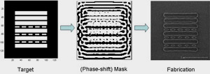
Optical microlithography, a technique similar to photographic printing, is used for transferring circuit patterns onto silicon wafers. A typical process consists of carving out the desired wafer pattern on a photo-mask (reticle), and projecting its image onto a chemically sensitive material (photo-resist), which acts as a recording medium.
However, the above process introduces distortions arising from optical limits and non-linear resist, and the output wafer pattern has poor pattern fidelity. With circuit dimensions already reduced to 65nm, and exponentially decreasing further in accordance with Moore’s law, the above problem becomes very critical.
One way of correcting the above process is by modifying the mask,
thereby changing the amplitude and phase of the wave-front, such
that it cancels out or compensates for the process losses to
come. This forms the basis of computational lithography.
Related Journal Publications
- A. Poonawala, Y. Borodovsky, P. Milanfar “Double Exposure Inverse Lithography”, Microlithography World, 16 (4): 7-9 Nov. 2007.
- A. Poonawala, P. Milanfar, “A Pixel-Based Regularization Approach to Inverse Lithography”, Microelectronic Engineering, 84 (2007) pp. 2837–2852
- A. Poonawala, P. Milanfar, “Double Exposure Mask Synthesis using Inverse Lithography"”, J. Micro/Nanolith. MEMS MOEMS 6(4), 043001, Oct–Dec 2007
- A. Poonawala, P. Milanfar, “Mask Design For Optical Microlithography—An Inverse Imaging Problem”, IEEE Trans. on Image Processing, vol. 16, no. 3, pp. 774-788, March 2007.
Related Conference Publications and Presentations
- A. Poonawala, Y. Borodovsky, and P. Milanfar, “ILT for Double Exposure Lithography with Conventional and Novel Materials”, Proceedings of the SPIE Advanced Lithography Symposium, February 2007.
- A. Poonawala, and P. Milanfar, “OPC and PSM design using inverse lithography: A non-linear optimization approach”, Proc. of the SPIE Conference on Optical Microlithography XIX, San Jose, February 2006.
- A. Poonawala, and P. Milanfar, “Prewarping Techniques in Imaging: Applications to Nanotechnology and Biotechnology”, Proceedings of SPIE Vol. 5674, SPIE Electronic Imaging, Conference on Computational Imaging III, San Jose, CA, January 2005.